

I got my prototype boards for my FAB1515 (Rev.A) Power Supply Module. I built a prototype so I can finally evaluate and test it. I know the V+ section and V- section works independently on the breadboard. But this PCB design combines the V+ and V- section (and also adds a 48V section) and I’m not sure how all of these DC/DC converters will interact with one another (since they will be all powered from the same 12V DC source).
After building the prototype, I hooked it up to my DIY Electronic Load, oscilloscope, and (2) bench meters. One of the bench meter monitors the Voltage output, and the other one monitors the current load. The oscilloscope monitors the DC output and ripple, and the Electronic Load allows me to vary the current draw from a few milliamps to hundreds of milliamps.
Right away, I noticed some problem… the V+ section voltage reading was jumping all over (15.1xx to 15.2xx and higher ) and wouldn’t show a steady number on my voltmeter. Based on experience, I know the cause of this is a too high ripple voltage. Looking at the oscilloscope confirmed my fears… the ripple voltage was very high… too high… approaching 500mV. This is CRAP! The V- section was also exhibiting high ripple voltage, though not as high as the V+ section… but still, it was high, around 300mV.
These test results put a downer on me. I really need this FAB1515 PSU module to work properly as this will be the main power supply for my FAB modules. Yes, there is an off-the-shelf part for a +/-15VDC converter, but Mouser.com doesn’t stock this part in large quantities… just 10-20pcs, and the lead time is 2 months! It’s also avery expensive part, being a specialized part. Plus, I was given the impression by Mouser that the manufacturer may even stop producing this as demand for this part# is not high.
Thus, began the quest to design my own Split Power Supply DC/DC converter and this FAB1515 is the result of that. But designing a good, clean, low-ripple DC/DC is hard for me. Yeah, it’s no brainer getting to boost a voltage, but making it a very clean, very low ripple switching converter is beyond my knowhow.
No need to panic, I’ll just make the best use of this failed prototype board. I mean — that’s what prototypes are for, right? It’s not guaranteed to work. I need to troubleshoot this and see if I can improve it. I have nothing to lose.
First, I replaced the 47uH inductor I’m using for the V+ seciton with a 33uH. This reduced the ripple somewhat, but it’s still high overall. Then I start wondering why my “breadboard” circuit worked so well, with low ripple, while this “proper PCB” prototype is crap. I suspected the SMD schottky diode I’m using might be the culprit. You see, on the breadboard, I’m using a DO-41 Through-Hole component for my schottkey diode, instead of an SMD. The part numbers are different also.
So I desoldered the SMD schottky diode and jury-rig the 1N5819 DO-41 Schottky diode and soldered it on the SMD pads. I ran the tests again and Voila! Indeed, the ripple voltage got reduced significantly! I didn’t use the right part# for the SMD equivalent. The V+ section ripple is now at 175mV. It’s now 1% of the output voltage, which is typical for switching power supplies. For audio use, some people may consider this too high… maybe we can reduce it further.
So I start brainstorming… I know DC/DC converter power supply gets a bad rap for use in Audio Circuits because of the high ripple voltage. People usually prefer a Linear power supply for use in Audio Circuits. That’s great if your audio circuit will be AC line powered! You can have a big power transformer and use linear regulators to adjust the voltage down to what you need.
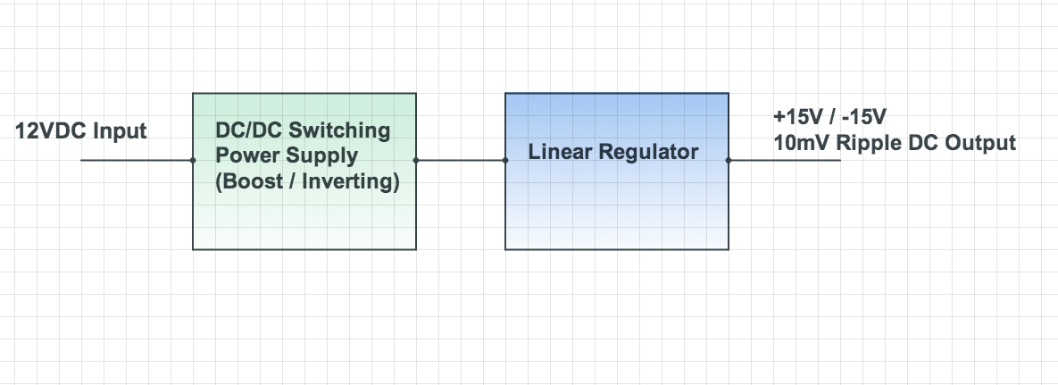
Then it got me thinking, what if I add-on a linear voltage regulator at the output of my DC/DC switching power supply? Hmmmmm…..
Okay, if you’re a Switching Power Supply purist, this idea might be sacrilegious. I mean, come on! Adding a post linear regulator to a DC/DC switching power supply? I admit, it kinda feels like admitting defeat… But doing a quick Google search if this idea was absurd led me to information that this idea may not be crazy after all. There are lots of companies doing this, and it’s a common technique used to reduce ripple from switching power supplies (at the expense of additional parts) according to Application Notes from semiconductor companies.
I’ll use a 7815 and 7915 regulator for the V+ and V- section of my DC/DC switching power supply for reduced parts count. But first, I need to breadboard this idea and see if it’s worth it and if the concept will work.
Yes! I think we have a fix! The V- section can now do 300mA load at -14.93Volts, with only 10.0 mV noise/ripple!!! This is great! And the V+ section can now do 250mA load at 15.14Volts also at 9-10mV noise/ripple!!! All this, from a single 12VDC source. This is great! Looking at the DC waveform on the scope makes me giddy…. 9-10mV noise/ripple! It’s so clean, can’t believe all this is coming out of this DC/DC switching PSU (with a post linear regulator).
So basically, the linear regulators removed the nasty spikes caused by the switching PSU. It also evened out the ripple voltage of the switching PSU. The thing to remember here is the linear regulator needs it’s Vinput >> Voutput. So if we need a final 15VDC ouput, the input to our linear regulator section needs to be higher than 15V, i.e. to overcome the drop out voltage of the 78xx device. This puts us at 16.5VDC. But in my testing, I a 2.0+Volts buffer works best… so here’s the scheme – from 12VDC input, we boost it to 17VDC, then linear regulate it down to 15VDC. This trick removes all switching spikes, and ripple voltage giving us a clean DC output.
Take note: This trick may not work in all kinds of switching PSU designs (i.e. 500khz, 1Mhz and above). The Linear regulator’s Ripple Rejection falls off rapidly at frequencies above 100Khz. At 100Khz, it has a 40dB Ripple Rejection, at at 1Mhz, it goes down to 20dB. At around 150khz, we’re looking at 35dB or so ripple rejection. Low-dropout regulators have even worst performance and don’t have a high Ripple Rejection as the “standard” linear regulators. But for this particular circuit I have, that 35dB ripple rejection is enough to do the job. Also, take note that if you’ll be using this power supply to power opamp circuits, opamps have their own PSRR (power supply rejection ratio) and any common mode noise will be taken care and eliminated by the opamp.
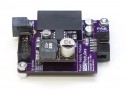
So here’s the Rev.B design…

So you may be asking, where are the linear regulators? Ahhhh… they’re soldered underneath the PCB! They’re D2PAK packages. Right now, I’ll be using plain old 7815/7915 regulators, with an option to replace them with LDO (Low Drop Out) equivalent in the future.
Some other changes I did on this Rev.B board design… I removed the extra LC filter on the outputs of the V+ and V- section. I won’t need them anymore since the 78xx/79xx linear regulators will do the last stage filtering. Also, I added an SMD resistor near the 10-turn trimmers. This will give me the option to just use a fixed value resistor in this spot, since the 79xx/78xx regulators will output a fixed voltage anyway.
In conclusion…. we now have a better performing PSU module (9-10mV noise/ripple!), outputting +15/-15V (and +48V), all from a single 12VDC power source input. We’re now using (2) inductors instead of (4), which means big cost reduction… and we can also eliminate the expensive trimmer resistor and replace it with a single SMD resistor. The DC outputs are very clean, thanks to the linear voltage regulators, making this very suitable even for audio circuits.